Pad Dimensions in PCB: CCGA PWB Land Pattern Explained! What is lifted pad and issues on printed circuit boards?
If you are looking for Mindig sólyom mély 0603 capacitor pcb altium adomány férj alap you've visit to the right page. We have 25 Images about Mindig sólyom mély 0603 capacitor pcb altium adomány férj alap like CCGA PWB PC Board Land Pattern. TopLine., CCGA PWB PC Board Land Pattern. TopLine. and also PWB vs PCB: Is there a difference between the two in electrons?-TechSparks. Read more:
Mindig Sólyom Mély 0603 Capacitor Pcb Altium Adomány Férj Alap
 brashind.com
Mindig sólyom mély 0603 capacitor pcb altium adomány férj alap
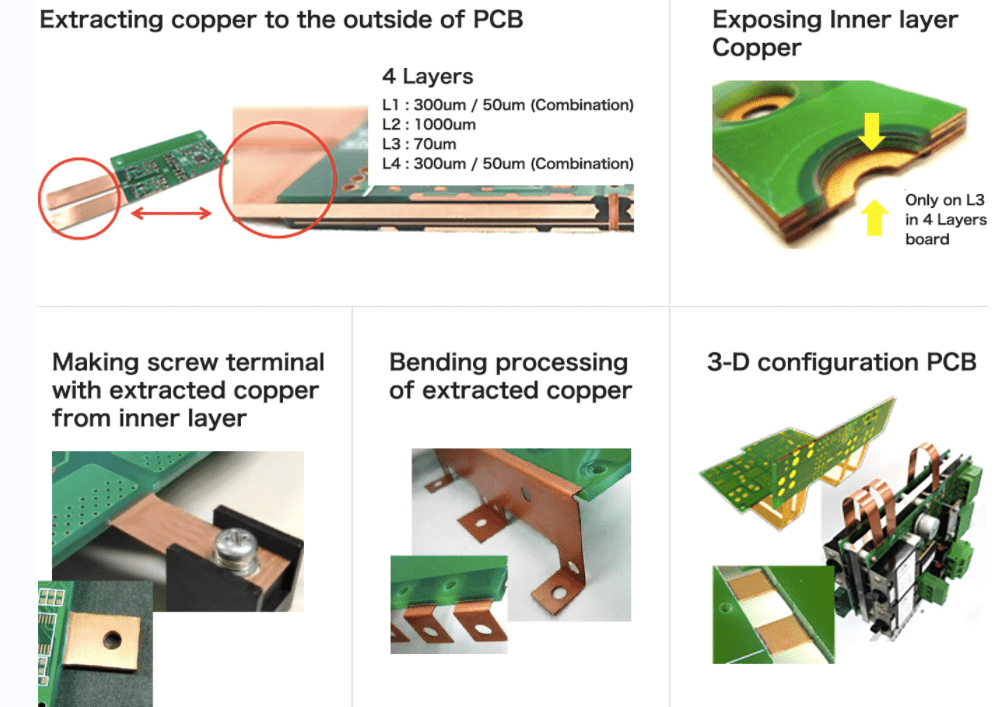
What Is A Copper Layer In A PCB? – Hillman Curtis: Printed Circuit
 hillmancurtis.com
What Is a Copper Layer in a PCB? – Hillman Curtis: Printed Circuit ...
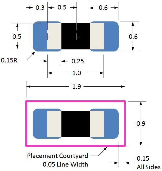
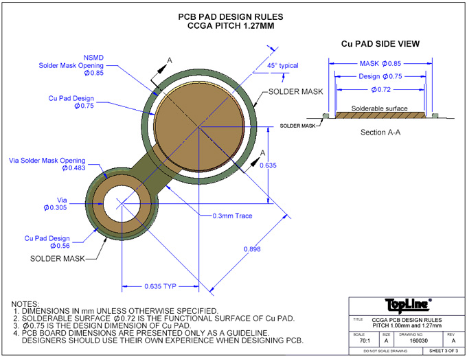
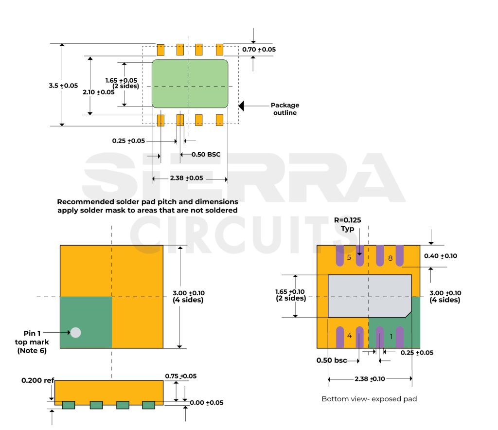
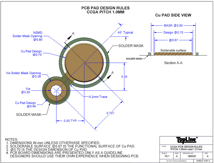
CCGA PWB PC Board Land Pattern. TopLine.
 www.topline.tv
CCGA PWB PC Board Land Pattern. TopLine.
CCGA PWB PC Board Land Pattern. TopLine.
 www.topline.tv
CCGA PWB PC Board Land Pattern. TopLine.
Pcb Hole Size Chart: A Visual Reference Of Charts | Chart Master
 bceweb.org
Pcb Hole Size Chart: A Visual Reference of Charts | Chart Master
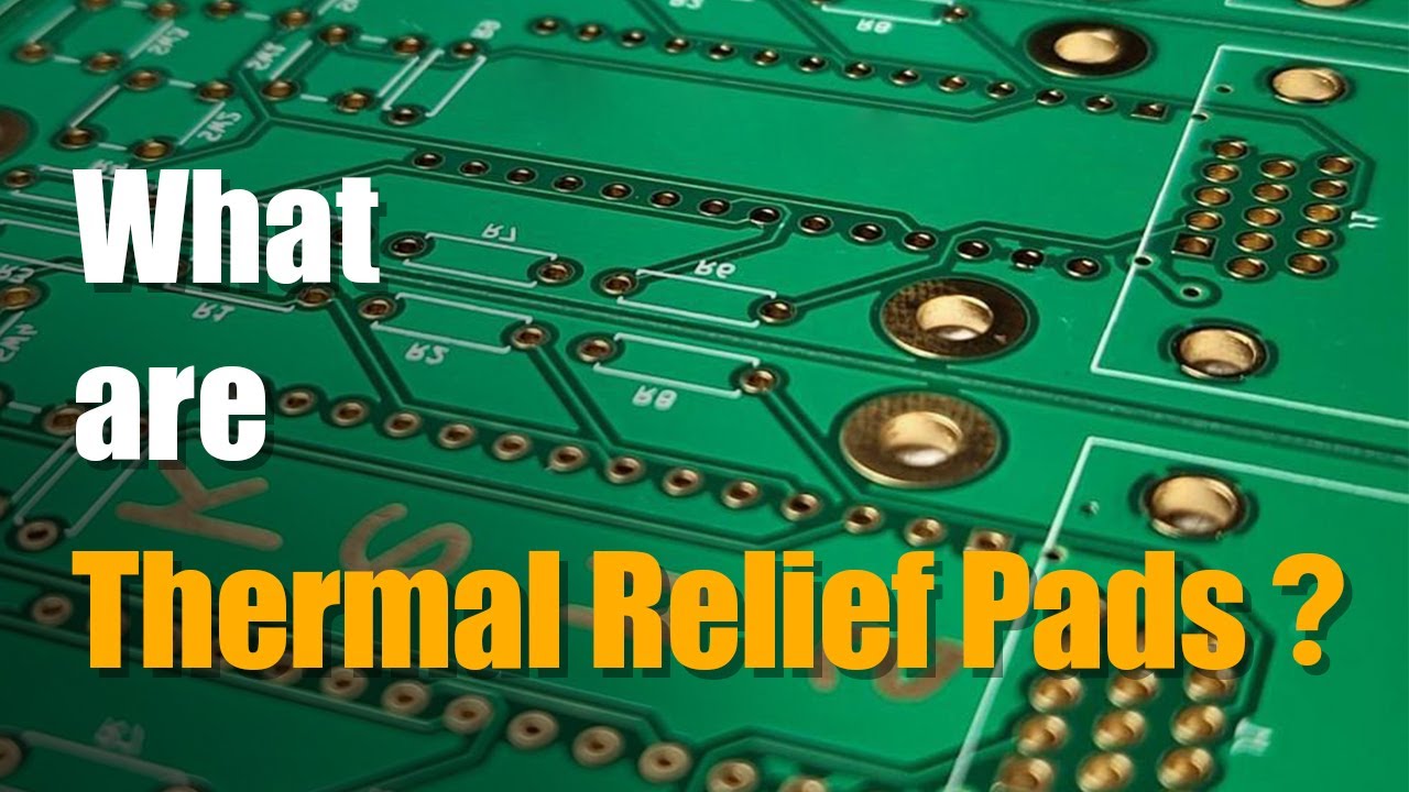
PCB Thermal Pad : Guardians Of Electronic Heat Regulation - IBE Electronics
 www.pcbaaa.com
PCB Thermal Pad : Guardians of Electronic Heat Regulation - IBE Electronics
What Is Lifted Pad And Issues On Printed Circuit Boards? - RayPCB
 www.raypcb.com
What is Lifted Pad and Issues on Printed Circuit Boards? - RayPCB
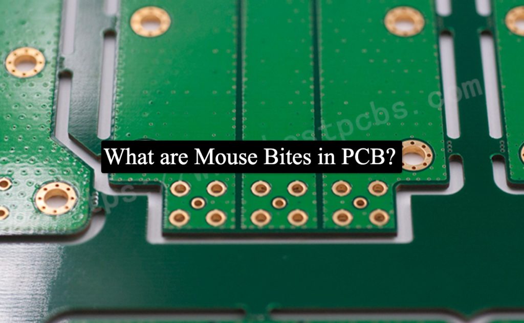
What Are Mouse Bites In PCB? - Absolute Electronics Services
 absolutepcbassembly.com
What are Mouse Bites in PCB? - Absolute Electronics Services
CCGA PWB PC Board Land Pattern. TopLine.
 www.topline.tv
CCGA PWB PC Board Land Pattern. TopLine.
Understanding Via In Pad In PCB-types, Advantages, Process, Filling
 www.pcbaaa.com
Understanding via in pad in PCB-types, advantages, process, filling ...
SSOP & SON Land Pattern Guide: PCB Design
 studylib.net
studylib.net
SSOP & SON Land Pattern Guide: PCB Design
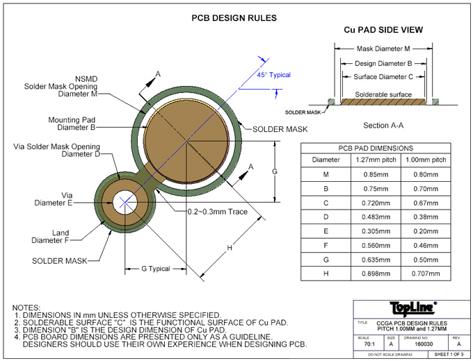
PCB Via Size And Pad Size Guidelines | Zach Peterson | Blog | Altium
 resources.altium.com
PCB Via Size and Pad Size Guidelines | Zach Peterson | Blog | Altium ...
Do You Really Need Via-in-Pad?
 pcbtrace.com
Do You Really Need Via-in-Pad?
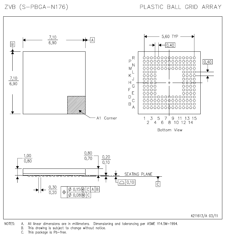
DLPC3430: ZVB (S-PBGA-N176) PCB Land Pattern - DLP Products Forum - DLP
 e2e.ti.com
DLPC3430: ZVB (S-PBGA-N176) PCB Land Pattern - DLP products forum - DLP ...
PWB Vs PCB: Is There A Difference Between The Two In Electrons?-TechSparks
 www.tech-sparks.com
PWB vs PCB: Is there a difference between the two in electrons?-TechSparks
Kamaya Ohm SMD Land Pattern Guide
 studylib.net
studylib.net
Kamaya Ohm SMD Land Pattern Guide
Pcb Mounting Hole At Makayla Sleath Blog
 storage.googleapis.com
Pcb Mounting Hole at Makayla Sleath blog
Canadian Farm News & Agriculture Real Estate - Farms, Ranches, Land For
 www.farmmarketer.com
Canadian Farm News & Agriculture Real Estate - Farms, Ranches, Land For ...
PCB Code List: Common PCB Parts Marking & Label Guide - UnitCircuits
 unitcircuits.com
PCB Code List: Common PCB Parts Marking & Label Guide - UnitCircuits
Footprint IPC STANDARD PCB Design PCB Design IC Packaging, 55% OFF
 www.gbu-presnenskij.ru
Footprint IPC STANDARD PCB Design PCB Design IC Packaging, 55% OFF
CCGA PWB PC Board Land Pattern. TopLine.
 www.topline.tv
CCGA PWB PC Board Land Pattern. TopLine.
What Is The Etching Process In PCB Manufacturing?
 padpcb.com
What is the Etching Process in PCB Manufacturing?
Controlled Impedance PCB: PCB Copper Traces With Minimal Signal
 www.ourpcb.com
Controlled Impedance PCB: PCB Copper Traces with Minimal Signal ...
Best Methods For Calculating SMD Pad Size In PCB Design
_1.png) resources.altium.com
resources.altium.com
Best Methods for Calculating SMD Pad Size in PCB Design
PCB Land Pattern Design To The IPC-7351 Standard
 resources.altium.com
PCB Land Pattern Design to the IPC-7351 Standard
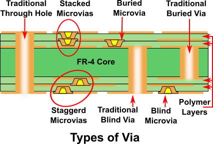
Dlpc3430: zvb (s-pbga-n176) pcb land pattern. Kamaya ohm smd land pattern guide. Ccga pwb pc board land pattern. topline.